KEEVAN HAROLD / ELECTRICAL ENGINEERING

From logic.
To layout.

I’m an electrical engineering student at Waterloo, working across digital hardware, PCB design, and the software that puts systems to the test.

Explore my work ↓

Toronto, ON University of Waterloo · BASc ’29

01 / BOARD STUDYFRONT COPPER
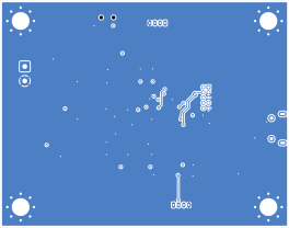
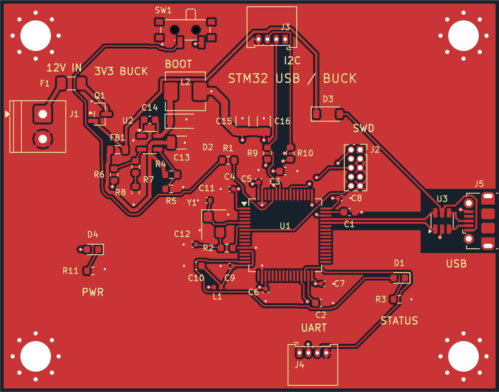
Actual KiCad front-copper layout of Keevan’s STM32 USB and buck-converter board
STM32 USB / BUCK4 LAYERS · 3.3 V

SELECTED WORK

01—02
01

DIGITAL DESIGN / VERIFICATION

A processor, one cycle at a time.

RISC-V CPU

Single-cycle RISC-V processor

A modular SystemVerilog core implementing an RV32I subset, from arithmetic and memory access to branches and jumps. Seven self-checking testbenches connect individual logic blocks to end-to-end program execution.

SystemVerilogIcarus VerilogMakeSurfer
32-bit
RISC-V datapath
7
Self-checking testbenches
14
Smoke-test cycles

01A / ARCHITECTURE

Following an instruction through the core

Open diagram ↗

The datapath connects instruction fetch, register operands, execution, memory access, and writeback. Separate branch logic decides when execution leaves the sequential PC + 4 path.
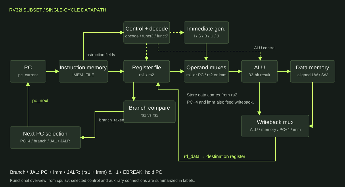
CPU datapath: PC to instruction memory, register file, operand muxes, ALU, and data memory. A writeback mux returns results to registers, while branch logic controls the next PC.
Simplified from the actual SystemVerilog connections. This is a single-cycle core, not a pipeline.

Flexible operands

Input muxes select a register or the PC for operand A, and a register or immediate for operand B. That supports register arithmetic, address generation, and AUIPC using the same ALU.

Four writeback sources

The destination register receives an ALU result, loaded memory word, PC + 4 link address, or upper immediate. JALR clears the target’s least significant bit.

01B / VERIFICATION

A smoke test, explained signal by signal

Open annotated trace ↗

These signals come directly from the saved simulation trace. Highlighted intervals connect memory operations and control flow to the program counter’s actual progression.
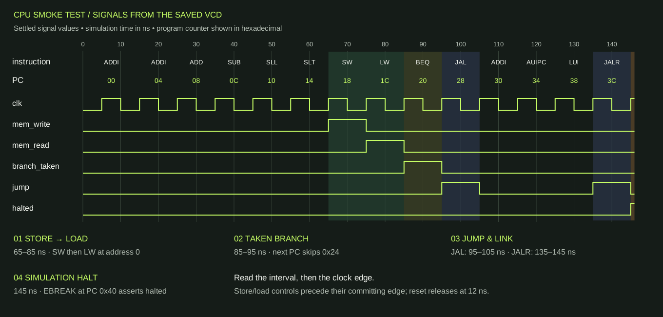
Annotated VCD waveform: store from 65 to 75 ns, load from 75 to 85 ns, taken branch from 85 to 95 ns, JAL from 95 to 105 ns, JALR from 135 to 145 ns, and EBREAK halt at 145 ns.
Redrawn from cpu_core_smoke.vcd. Times are simulation times, not measured hardware performance.

Memory and branch behavior

The test checks that a store writes 8 to memory word 0 and the following load returns 8 in x7. The taken BEQ skips PC 0x24, leaving x8 unchanged.

Links and a deterministic endpoint

The test checks link values of 44 in x9 for JAL and 64 in x13 for JALR. EBREAK at PC 0x40 raises halted; this is a simulation completion interface, not trap handling.

View original waveform screenshot ↗
Inside the design +

Architecture

Program counter, instruction memory, register file, immediate generator, ALU and control, branch unit, data memory, and writeback mux. Parameterized instruction loading and deterministic reset make simulation repeatable.

Verification & scope

Checks cover arithmetic, signed comparisons, aligned LW/SW, control flow, and reset. EBREAK provides a simulation-only halt. This educational core implements an RV32I subset; FPGA synthesis and full ISA compliance are future work.
02

PCB DESIGN / POWER ELECTRONICS

Power and signals, on four layers.

STM32 PCB

STM32 USB & buck-converter board

A four-layer KiCad design combining an STM32 controller, USB, and 3.3 V buck regulation. The layout brings together power routing, local decoupling, a ground reference plane, and I2C, UART, and SWD interfaces.

KiCad4-layer PCBSTM32Power integrity
4
Copper layers
3.3 V
Buck regulation
0
Reported DRC violations

02A / BOARD WALKTHROUGH

Six places where the layout matters

Open full board ↗
Front copper of the STM32 board, with numbered regions corresponding to the adjacent explanations123456
Actual routed front-copper export with numbered design callouts.
  1. Buck power stage

    The regulator, inductor, and local capacitors sit together. Wider copper is used for the power path, with short local switching connections.

  2. STM32 at the center

    The MCU sits between the supply, USB interface, oscillator, and headers, keeping critical support circuitry close.

  3. USB interface

    D+ and D− stay on the front copper. The routed pair uses a ground reference underneath; final impedance still needs manufacturer confirmation.

  4. External crystal

    The crystal and load capacitors sit beside the MCU to keep oscillator connections local.

  5. Local decoupling

    Capacitors near the supply pins provide local charge storage, with ground connections tied into the reference plane.

  6. Debug and peripheral access

    SWD is at the right of the MCU, I2C at the top edge, and UART at the bottom, separating external access from the central circuitry.

02B / COPPER STACK

A role for every layer

TOP → BOTTOM

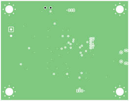
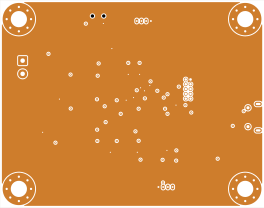
Four copper layers separate critical surface routing from ground and power distribution. All views use the same top-side orientation so component and via locations line up.

KiCad export of F.Cu · Front signals
01

F.Cu · Front signals

USB and critical local routes share the component side with ground pours.

KiCad export of In1.Cu · Ground reference
02

In1.Cu · Ground reference

A continuous ground plane provides a nearby return reference, interrupted by required hole and via clearances.

KiCad export of In2.Cu · 3.3 V distribution
03

In2.Cu · 3.3 V distribution

The internal supply plane distributes the regulated 3.3 V rail across the board.

KiCad export of B.Cu · Bottom signals
04

B.Cu · Bottom signals

Selected crossing signals use the bottom layer, alongside a filled ground pour.

Routed review draft: the saved KiCad checks report zero DRC violations and unconnected items. These views document the design; fabrication and electrical testing are still pending.

Layout decisions & status +

Routing strategy

Front copper carries USB and critical local connections, with selected crossings on the bottom. Internal layers provide ground and 3.3 V. Short decoupling connections and broad power traces support the supply layout.

View full board layout ↗

Routed review draft

The saved KiCad report records zero design-rule violations, unconnected items, or schematic parity issues. Fabrication and electrical testing are not yet complete. Component selection, USB power behavior, and manufacturing impedance still need final review.

Learning project based on Phil’s Lab #11.

BEHIND THE WORK

Hardware curiosity.
Software experience.

I’m pursuing a BASc in Electrical Engineering at the University of Waterloo, expected in 2029. My experience spans rail-system test automation, C++ development, and data science.

My toolkit

SystemVerilog · VHDL · C++ · Python
KiCad · Quartus Prime · Git · Postman
Icarus Verilog · Make · Surfer

MAY—AUG 2026 / SEP—DEC 2025

Hitachi Rail

Software Analyst · Co-op

Developed C++ test-data viewer features, including filtering and event timelines. Built Python automated tests and REST API checks against CBTC system requirements.

APR—AUG 2024

Swarmio

Junior Data Scientist

Supported latency and edge-computing tests for gaming applications, preparing Python datasets for CreateML and CoreML experiments.

Read my full résumé ↗

GET IN TOUCH

Let’s build something
worth testing.

keevan.harold@gmail.com ↗